")
Application Specific Integrated Circuits, or ASICs, are special-purpose integrated circuits that are created and manufactured to meet particular user requirements as well as the needs of a particular electronic system.
Learn more about ASIC chips by continuing to read.
What is An ASIC Chip?
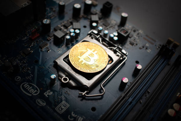
ASIC (Application Specific Integrated Circuit ) chip is a dedicated integrated circuit, a proprietary application chip designed and manufactured from the root level in response to user requirements for a specific electronic system, whose computing power and computational efficiency can be customized according to algorithm needs, and is the product of fixed algorithm optimized design. ASIC chip modules can be found in many different intelligent terminals, including artificial intelligence devices, virtual currency mining devices, consumable printing devices, and military defense devices.
At the hardware level, ASIC chips are composed of basic silicon materials, gallium phosphide, gallium arsenide, gallium nitride, and other materials. ASIC chip modules are assembled from IP cores like external storage units, power managers, audio screen processors, and network circuits at the level of the physical structure. To fulfill one or more specific needs, the same chip module can hold one or more ASIC chips with the same or different functions.
ASICs are distinguished by their user-specific requirements and offer benefits such as reduced size, reduced power consumption, increased reliability, improved performance, enhanced confidentiality, and lower cost when compared to general-purpose ICs produced in large quantities.
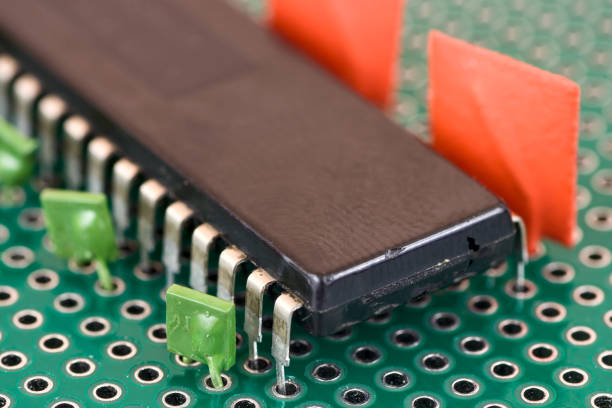
An integrated circuit is a miniature electronic device or component. Using a certain process, the transistors, resistors, capacitors, and inductors required in a circuit and wiring are interconnected together, made in one or several small semiconductor wafers or dielectric substrates, and then packaged in a shell, becoming a microstructure with the required circuit function. Since every part of the structure is whole, electronic parts are moving toward miniaturization, low power consumption, intelligence, and high reliability. In the 1970s, Jack Kilby and Robert Noyes developed integrated circuits based on silicon (Si) and germanium (Ge), respectively.
It is more challenging to set up a system for special requirements to change to address these issues the larger the integrated circuit scale. In order to achieve the best design for the entire system, superior performance, and confidentiality, special-purpose integrated circuits (ASICs) with user participation in design have emerged. On a single chip, ASICs are able to combine the functions of a number of general-purpose medium- and small-scale integrated circuits. In order to meet system requirements, the entire system can be integrated onto a single chip. It optimizes the entire circuit. Component count decreased, the wiring was condensed, volume and weight decreased, and system dependability increased.
ASIC Chip Design Process
To begin with, the ASIC must be separated into internal functional modules, each of which must implement a different function. The entire ASIC circuit is created by connecting each functional module to the others. In order to create register transfer level (RTL) code that satisfies the functional and interface requirements, the logic design of the modules is carried out in hardware description language (HDL). Third, write test code or test stimulus using a field-programmable logic gate array (FPGA) prototype or software simulation to check the logic and make sure the logic design complies with the ASIC specification’s functional and timing requirements. Fourth, the logic synthesis tool maps the RTL code to the corresponding process library. After completing timing verification and convergence, layout, wiring, and other layout designs are carried out to create the layout data for die production.
ASIC Chip Features
Advantages
① Area advantage: Repetitive logic, processing, register, storage, and other architectures are avoided in ASIC chips. They are constructed as pure digital logic circuits, which helps to minimize the chip area. Small-area chips can be handled by cutting out more chips from a single wafer of the same size, which enables businesses to save money on wafer costs.
② Energy consumption advantage: ASIC chips use less power per calculation compared to CPU, GPU, and FPGA. For example, while GPU uses about 0.4 watts of electricity per calculation, ASIC uses only about 0.2 watts, better meeting the energy requirements of new smart home appliances.
③ Integration advantage: ASIC chip system, circuit, and process are highly integrated due to custom design, which helps customers to obtain high-performance integrated circuits.
④ Price advantage: influenced by the small size, high operation speed, and low power consumption, Compared to CPU, GPU, and FPGA chips, ASIC chips are significantly less expensive. The current average price of ASIC chips in the global market is about $3. In the long run, it is anticipated that the cost of ASIC chips will continue to drop once mass production is achieved.
Disadvantages
① ASIC chips require extensive customization, lengthy design and development cycles, and physical design and reliability verification on the final products.
② Algorithms are heavily reliant on ASIC chips. Artificial intelligence algorithms are updated and iterated at high speed, resulting in a high update frequency of ASIC chips.
③ The likelihood of ASIC finished products being discontinued from the market increases due to the high level of customization found in ASIC chips and the lengthy R&D cycle.
Classification of ASIC Chips
According to the Degree of Customization
① Full-custom ASIC Chips
One of the most customized chips is full-custom ASICs, where programmers design logic units for various functions based on various circuit structures and construct analog circuits, memory cells, and mechanical structures on the chipboard. The ASIC chip mask boards are also highly customized, and they serve as the connection between the logic cells.
Full-custom ASIC chips are expensive to design, taking more than nine weeks on average for each chip module. For advanced applications, this kind of chip is frequently used.
Full-custom ASIC chips are more efficient and consume less power than semi-custom ASIC chips. A full-custom ASIC chip’s average arithmetic output is roughly 8 times higher for the same function than a semi-custom ASIC chip’s average arithmetic output under the same process, and a full-custom ASIC chip with a 24nm process performs better than a semi-custom ASIC chip with a 5nm process.
② Semi-custom ASIC Chips
The majority of the logic cells used in semi-custom ASICs are drawn from the standard logic cell library, but some of them are specially created to meet particular needs. Compared to a fully customized ASIC chip, there is a lower design cost and more flexibility.
Depending on the number of standard logic cells and custom logic cells, semi-custom ASICs can be subdivided into gate array chips and standard cell chips.
③ Programmable ASIC Chip
Programmable ASIC chips can be divided into FPGA chips and PLD chips. In actual production, the number of research institutions and companies that classify FPGA chips as different from ASIC chips is increasing, so this report only considers PLD (Programmable Logic Device) as a subcategory of programmable ASIC chips.
PLDs also referred to as programmable logic devices, are made up of a matrix of flip-flops, latches, and other basic logic components. in their structure, and their interconnected parts exist as individual modules. Designers can program PLDs to meet some of their custom application requirements.
According to the Terminal Function
Depending on the terminal function, ASIC chips can be categorized as TPU chips, BPU chips, or NPU chips.
① Tensor processors called TPUs are specifically designed for machine learning. As an illustration, Google created an internal instruction set for a programmable AI accelerator for the Tensorflow platform in May 2016. This accelerator runs whenever the Tensorflow program updates or changes its algorithms.
② The embedded AI processor architecture that Horizon Technology has suggested is called BPU, or “Brain Processor.”
③ Using a deep learning instruction set, the NPU is a neural network processor that directly processes massive amounts of electronic neuron and synapse data while simulating human synapses and neurons at the circuit layer.
ASIC Chip Products Introduction
① The Google Cloud TPU platform and machine-learning supercomputer can be supported by the TPUs that are built into the 2017 version of Google’s AlphaGo physical processor, which has four of them. TPU was first introduced by Google in 2016.
② In August 2014, IBM released the second-generation TrueNorth chip with a 28nm process, which simulates brain structure and can be used for real-time video processing.
③ In 2017, Intel released the Xeon family of ASIC chips. Without the aid of additional host processors and auxiliary processors, this series of chips can function as a standalone processor for machine deep learning.
④ Stanford University introduced ASIC chips based on a new neuromorphic computing architecture with a computing speed of 9,000 times that of an ordinary computer, which can simulate about 1 million brain neurons and billions of synaptic connections.
⑤ ASIC chips are increasingly being used in security, assisted driving, conventional home appliances, smart medical, and other fields, according to emerging science and technology firms.
Summary
The ASIC chip is a fixed algorithm-optimized dedicated integrated circuit (ASIC), a proprietary application chip designed and produced from the ground up in response to user requirements for a particular electronic system. The ASIC chip’s computing power and computational efficiency can be customized in accordance with algorithm needs. Artificial intelligence devices, virtual currency mining devices, consumable printing devices, military defense devices, and other intelligent terminals can all make use of ASIC chip modules.
FAQ
What Are ASIC Chips Used For?
The uses for ASICs vary widely, but all generally involve controlling how an electronic device will function. From communications satellites, avionics, and artificial intelligence to digital watches, cell phones, and toys with electronics.
Can the ASIC Chip Be Programmed?
ASIC in VLSI stands for application-specific integrated circuits. This integrated circuit is aptly named since an ASIC microchip is designed and manufactured for one specific application and does not allow you to reprogram or modify it after it is produced.
What Are Examples of ASIC Chips?
Examples of ASIC Ics include a chip for a talking toy bear, a satellite, a chip that manages the memory-to-microprocessor interface for a workstation CPU, and a chip that houses a microprocessor as a cell along with other logic.